
一,Structural Design Principles: Transitioning from Mechanical Models to Functional Integration
1. Three-dimensional honeycomb structure: the main way that energy is lost
Chips and optical lenses are two examples of high-precision electronic products that are very sensitive to impact energy. The biomimetic honeycomb structure architecture of moulded pulp spreads impact energy to many separate units. For instance, a brand of lidar packaging features hexagonal honeycomb cells that are 8mm long on each side and 0.5mm thick on the walls. The peak acceleration reduced from 1200g of regular EPS foam to 380g in the 1.2m drop test, which protected the internal precision structure.
Points of design:
Optimising the size of the unit: It is best to keep the honeycomb unit side length to product aspect ratio between 1:5 and 1:8 based on the weight and size of the item.
Design for a wall thickness gradient: To make the wall stiffer in that area, make it 0.8mm thick at the product side. To make it better at absorbing energy, make it 0.3mm thick on the outside.
Verification of dynamic simulation: Use LS-DYNA software to simulate a 1.5-meter drop and find the best angle for the honeycomb layout (typically 45° to the direction of impact).
2. Composite material reinforcement: going beyond the limits of pulp performance
The elastic modulus of typical pulp moulding is only 0.2–0.5 GPa, which makes it hard for heavy equipment like servers and industrial controllers to hold up. Adding nanocellulose (NCC) or carbon fibre (CF) reinforcement materials can raise the modulus to between 2 and 5 GPa. For instance, the battery packaging for the Huawei Mate 60 is made of composite pulp that is 30% glass fibre. The distortion in a 50kg stacking test is only 1.2mm, which is 76% less than pure pulp.
Designing a formula for materials:
Effect of adding a material class to the performance improvement ratio
The tensile strength of nano cellulose (NCC) goes up by 5–10% and the water absorption rate goes down by 30%.
Carbon fibre (CF) has a 15–20% higher elastic modulus and a 300% higher conductivity.
Bio-based resin with a temperature resistance of 5–8% was raised to 120 °C while still being biodegradable.
3. Integration of functional coatings: Making several barriers to safeguard
Static electricity, electromagnetic interference (EMI), and microbiological contamination can all cause problems with high-precision electronic products. Using surface coating technology, you can get the "anti-static+shielding+antibacterial" effect:
Add 2–5% carbon black or graphene to the surface to make it less resistant to electricity (10 ⁶–10 ⁹ Ω/sq), which meets the IEC 61340–5–1 standard.
Coating for electromagnetic shielding: Nickel-plated fibre (5 μm) composite covering that cuts weight by 60% compared to typical metal shielding and blocks 40dB of sound in the 1-18GHz frequency range.
Antibacterial coating: When treated with nano silver ions (Ag + concentration 50ppm), it stops more than 99% of Escherichia coli and Staphylococcus aureus from growing.
二, Key technological parameters: exact control from the lab to mass production
1. Making the settings for the moulding process work better
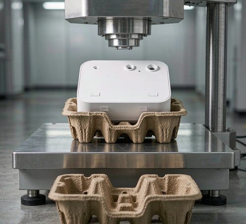
The mechanical properties of moulded pulp are directly affected by its density (0.4–0.8g/cm³). You can get very exact density control by changing the temperature (180–250 °C), pressure (5–10 MPa), and holding time (10–30 seconds) during the hot pressing process.
Low density (0.4–0.5g/cm ³): good for lightweight cushioning packages like cell phones and headphones. It can absorb up to 85% of the impact.
High density (0.6–0.8g/cm ³): utilised to support large machinery like servers and industrial robots. It can hold up to 15–20MPa of pressure.
The packaging for the Dell XPS 13 notebook has a gradient density design, with a density of 0.7g/cm³ in the bottom support area and 0.45g/cm³ in the top buffer area. The screen damage rate went down from 18% to 3% when the drop test was 1.5 meters.
2. Demoulding slope and fillet radius: Electronic devices that need to be very precise need packaging that is very precise (tolerance ± 0.1mm), and the demoulding slope and fillet radius must be strictly controlled.
Demoulding slope: The slope of the inner cavity is 1–3 °, while the slope of the exterior wall is 0.5–1 °. This keeps the product from getting stuck or the package from changing shape.
Rounding radius: R3-R5mm rounded corners are employed in the structure's transition to lower stress concentration (stress concentration factor lowered by 40%).
Verification of the simulation: Using ANSYS Workbench to model the demolding process and find the best slope and fillet combination, the mold's life was extended from 50,000 uses to 200,000 uses.
3. Collaborative design with several cavities
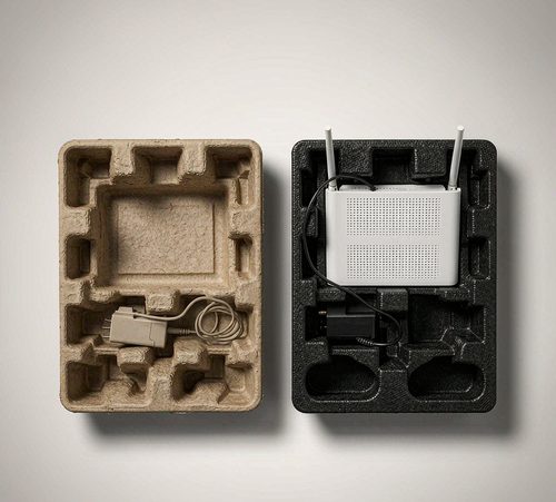
Multi-cavity design is needed for electronic devices with multiple parts (like drones and medical equipment) to have the right location and protection on their own:
Independent chamber: Each core part, like a chip or motor, has its own chamber that is ± 0.05mm in size to keep them from hitting each other while being moved.
Connecting channel: To keep the air pressure even and make it easier to open the box, put 0.5mm wide breathing openings between the chambers.
The DJI Mavic 3 drone comes in a case with 12 cavities, each with its own slot for the battery, gimbal, and blades. The rate of damage while unpacking has gone down from 3% to 0.2%.
三,A common use case is for consumer electronics and industrial equipment.
1. High-precision chip packaging: a solution that protects at the micrometre level
The packaging for 5nm process chips from a given brand must match these standards:
Not static: Surface resistivity is less than or equal to 10 ΩΩ/sq.
Moisture resistance: the rate at which it absorbs moisture must be less than 2% (in an atmosphere with 85% humidity for 48 hours).
Buffer: 1 metre drop: peak acceleration 500g
Answer:
Nanocellulose Reinforced Pulp (NCC 8%+Fiberglass 15%) is the material.
Structure: A double-layered honeycomb design with a 6mm side length on the top honeycomb and a 10mm side length on the bottom honeycomb.
Coating: Graphene anti-static coating (2 μ m thick) + Diatomaceous earth moisture-proof coating (5 μ m thick)
Results of the test:
Drop test: 1.2 meters down, 420g max acceleration
Test for moisture resistance: 85% humidity, 1.8% moisture absorption rate in 48 hours
Test for electrostatic energy: Surface resistivity: 6.2 × 10 ΩΩ/sq
2. Packaging for medical equipment: two problems to solve: keeping it clean and safe
The packaging for a portable ultrasound diagnostic instrument from a given brand must match these standards:
Aseptic requirement: Meets the medical grade standard ISO 11737-1
Buffer performance: A drop of 1.5 meters doesn't hurt it.
Environmental compliance: T Ü V Austria has confirmed that it is 100% recyclable and biodegradable.
Bamboo fibre (60%), bio-based resin (20%), and nano silver antibacterial agent (0.5%) make up the material.
Structure: a 3D mesh support and independent cavity location
covering: PLA biodegradable moisture-proof covering that is 8 μm thick
Results of the test:
Microbial testing: 99.9% of Escherichia coli and Staphylococcus aureus were stopped.
Drop test: 1.5 meters drop, 0.3 mm probe movement
Degradation test: After 180 days, industrial compost had a degradation rate of 92%.